Generate the Binary File format
FPGA Binary file can be generated, which will contain the following components:
FPGA Bitstream
FPGA MemInit (RAM Block Initialization)
FPGA IOMux Configuration
Then, FPGA bin [${TOP}.bin] == bitstream bin + meminit bin + iomux bin
We will need a header in the FPGA bin which indicates the component information (sizes).
The diagrams below show a complete picture of the FPGA bin structure.
FPGA bin header
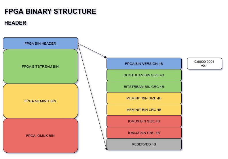
The header contains the fields:
FPGA BIN VERSION - which will help handle future changes in bin structure if needed. Currently at v0.1.
BITSTREAM BIN SIZE, CRC - size in bytes, and crc of the bitstream binary content
MEMINIT BIN SIZE, CRC - size in bytes, and crc of the meminit binary content
IOMUX BIN SIZE, CRC - size in bytes, and crc of the iomux binary content
RESERVED WORD - for future usage
FPGA bitstream bin
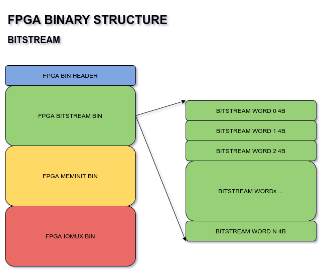
The bitstream bin will have 4B words, exactly as is currently generated in ${TOP}.bit
FPGA meminit bin
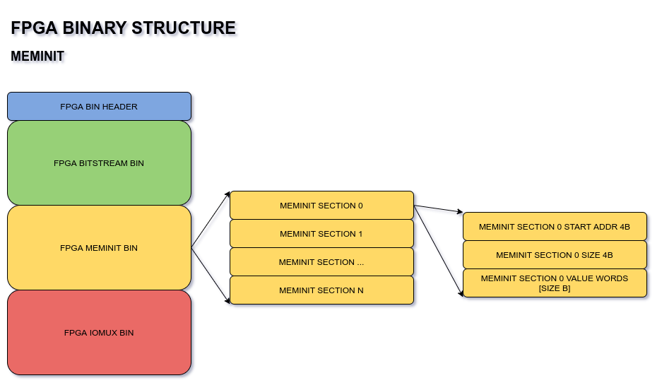
The meminit bin will have the same structure as is currently generated in the header method.
For each RAM block, we will have:
RAM block start address 4B
RAM block size 4B
size B of initialization values
This set will be repeated for as many RAM blocks intialized in the design.
FPGA iomux bin
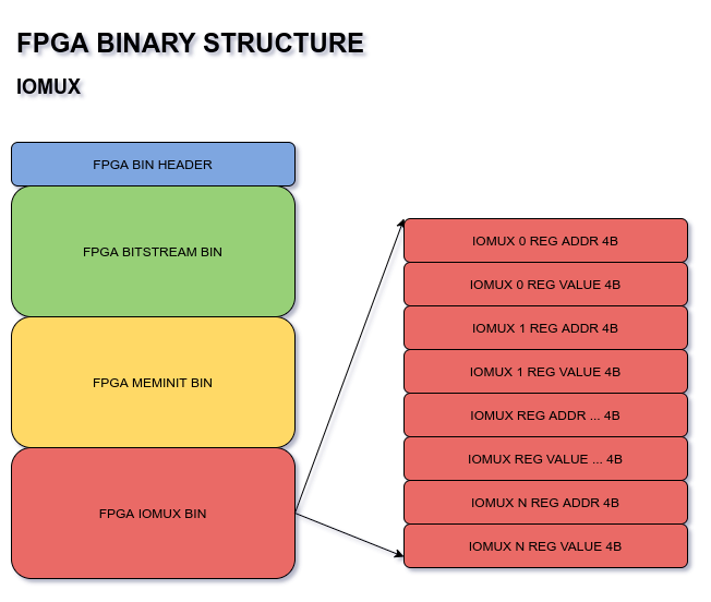
The iomux bin will have a set of pad configurations, each pad configuration is:
4B Reg Address
4B Reg Value
The number of pad configurations would be equal to the number of pads used by the FPGA design.
Syntax:
ql_symbiflow -compile -src <source complete path> -d <device> -t <top module name> -v <verilog files> -p <pcf file> -P <Package file> -s <SDC file> -dump binary
The output files dumped will be :
<TOP>.bin - file generated from the bit file input
ql_symbiflow -compile -src $PWD -d ql-eos-s3 -t top -v counter_16bit.v -p chandalar.pcf -P PD64 -s counter_16bit.sdc -dump binary
The generated binary file can then be flashed into the board with the programmer, and the bootloader can automatically can load the FPGA design.